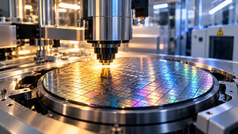
Inspection is becoming more important as advanced packaging moves toward smaller features, tighter spacing and more complex device stacks. In that environment, even minor voids, air gaps or delaminations can trigger electrical or mechanical failure later in the product life cycle.
Acoustic micro imaging (AMIacoustic micro imagingA non-destructive inspection method that uses high-frequency ultrasound to image internal structures and defects.) addresses these issues with high-frequency ultrasound. At the heart of the method is a transducer that converts electrical pulses into mechanical waves. Because ultrasound does not propagate through air, AMIacoustic micro imagingA non-destructive inspection method that uses high-frequency ultrasound to image internal structures and defects. can expose gaps and delamination that would otherwise be difficult to identify.
The choice of transducer depends on the sample and its frequency requirements. By moving the transducer across the device, the system generates multiple images that are evaluated in software. Based on the defect count, parts can then be accepted or rejected.
Typical defect signatures include visible air gaps, thinning of attach material on solder pads, and uneven solder or thermal interface material layers. When attach material becomes too thin, stress can promote delamination. Uneven TIMthermal interface materialA material placed between a heat source and a heat sink to improve thermal transfer. layers can also point to deeper problems in the build process.
AMIacoustic micro imagingA non-destructive inspection method that uses high-frequency ultrasound to image internal structures and defects. is often used alongside destructive testing and X-ray-based methods rather than as a full replacement. For development work, destructive tests can confirm proof of concept and verify that voids or delaminations detected by AMIacoustic micro imagingA non-destructive inspection method that uses high-frequency ultrasound to image internal structures and defects. are real before the method is integrated into production inspection.
The main technical distinction to transmission scanning is that AMIacoustic micro imagingA non-destructive inspection method that uses high-frequency ultrasound to image internal structures and defects. inspects layer by layer, while transmission methods and X-ray produce composite images. Both approaches are complementary, and composite images can be preferable for spherical structures such as ball grid arrays.
Increasing package complexity is pushing AMIacoustic micro imagingA non-destructive inspection method that uses high-frequency ultrasound to image internal structures and defects. software to handle new inspection tasks, including multi-die stacks instead of single flip chips. Machine learning is helping by distinguishing via patterns from true delamination, reducing false defect counts. Throughput is also a key pressure point: Nordson Test & Inspection has developed the automated SpinSAM tool, which can inspect four 300 mm wafers at once. Unlike raster scanning, SpinSAM keeps both wafer and transducer in continuous motion, improving throughput without image-stitching distortion.
As inspection requirements continue to rise, AMIacoustic micro imagingA non-destructive inspection method that uses high-frequency ultrasound to image internal structures and defects. is evolving from a straightforward defect-finding tool into a more automated and software-driven process for challenging package structures.