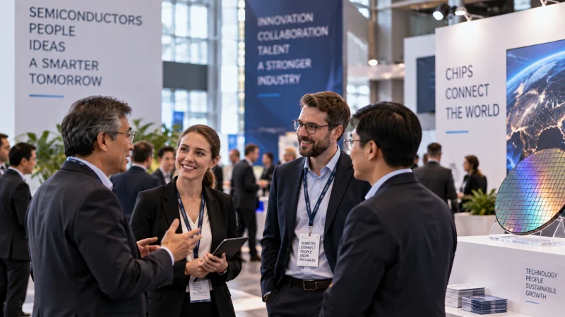
AIartificial intelligence workloads are pushing semiconductor packaging toward larger footprints and higher interconnect density, creating new demands on equipment makers. At A*STARsimultaneous transmitted and reflected’s Innovate Together 2026, participants focused on the packaging technologies and process capabilities needed to support that shift, with hybrid bonding, optical interconnects, and process control among the main topics.
The discussion centered on how packaging must evolve as AIartificial intelligence systems require more complex integration. Hybrid bonding was highlighted as one of the key approaches under review, alongside optical interconnects that can help address scaling pressures in dense assemblies. The emphasis on process control points to the need for tighter management of manufacturing steps as package complexity increases.
The event also underlined that these requirements are not isolated technical details but part of a broader packaging challenge. As AIartificial intelligence-oriented designs continue to demand more density and larger package structures, equipment suppliers face higher expectations for precision, integration capability, and control across the packaging flow.
In this context, the main issue is not a single device or process change, but the combined push toward more advanced assembly architectures. The result is a packaging landscape in which hybrid bonding, optical links, and process control become central factors for meeting AIartificial intelligence-driven integration needs.