Artificial intelligence is changing what the semiconductor industry has to deliver. The challenge is no longer limited to making a single chip faster or more efficient. Instead, the industry is being pushed toward complete computing systems that can deliver higher performance, move more data and consume less energy while still reaching market faster.
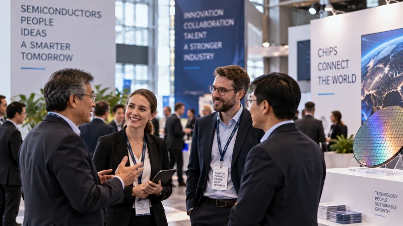
That message was central to the unveiling of Applied Materials’ EPIC1. Equipment and Process Innovation and CommercializationApplied Materials uses this name for its new collaborative R&D center.2. Electronics, Photonics and Integrated CircuitsEPIC names the collaboration center unveiled by Applied Materials. Center, where representatives from across the semiconductor ecosystem discussed the technical requirements of the AIartificial intelligence era. The companies involved included SK hynix, TSMCTaiwan Semiconductor Manufacturing CompanyTSMC is named as a founding partner of the EPIC Center., Micron, Intel, Samsung, Broadcom, NVIDIA and Qualcomm, alongside Applied Materials. Their presence underscored a common point: progress in one part of the stack is increasingly dependent on progress in others.
AIartificial intelligence workloads place heavy demands on processors, memory, interconnects, advanced packaging and power efficiency. Improving one element in isolation is no longer enough if another part of the system remains constrained. The bottlenecks are becoming interconnected across the entire technology stack.
Memory is one of the clearest examples. As AIartificial intelligence workloads expand, data movement between memory and compute becomes a major limit on both performance and energy use. High-bandwidth memory, tighter integration of memory and logic, and new packaging approaches are moving to the center of system design rather than being treated as a late-stage implementation detail.
Interconnects add another layer of difficulty. Large AIartificial intelligence systems split workloads across multiple processors, making communication speed, latency and energy consumption increasingly important. Advanced chip integration and co-packaged optics are among the approaches discussed as possible responses, but they depend on coordinated progress in materials, processes, packaging and system architecture.
Thermal management is also becoming more complex as more compute and memory are combined. The resulting heat problem cannot be treated separately from performance and efficiency targets. It is part of the same set of connected engineering constraints.
The event also highlighted the economic impact of this interdependence. If companies develop technologies independently and only integrate them late, integration issues can surface after substantial time and resources have already been spent. Earlier collaboration can expose constraints sooner, help evaluate trade-offs together and reduce the risk of delayed products and extra development cycles.
Applied Materials’ EPIC1. Equipment and Process Innovation and CommercializationApplied Materials uses this name for its new collaborative R&D center.2. Electronics, Photonics and Integrated CircuitsEPIC names the collaboration center unveiled by Applied Materials. Center is positioned as a response to that system-level challenge, with a focus on materials, processes and equipment for future semiconductor technologies. The broader point is that AIartificial intelligence is forcing innovation across the full stack, where performance, power, integration and manufacturability have to be considered together.