Foundries and OSAT1. Outsourced Semiconductor Assembly and TestA business model in which assembly and test services are provided by a specialized external supplier.2. outsourced assembly and testAn OSAT provider assembles, packages, and tests chips for other companies.s are increasingly blurring the boundary between front-end and back-end work. Foundries have long handled advanced-package back-end steps, but OSAT1. Outsourced Semiconductor Assembly and TestA business model in which assembly and test services are provided by a specialized external supplier.2. outsourced assembly and testAn OSAT provider assembles, packages, and tests chips for other companies.s are now taking on more of that activity as they acquire capabilities that resemble what foundries already do in packaging.
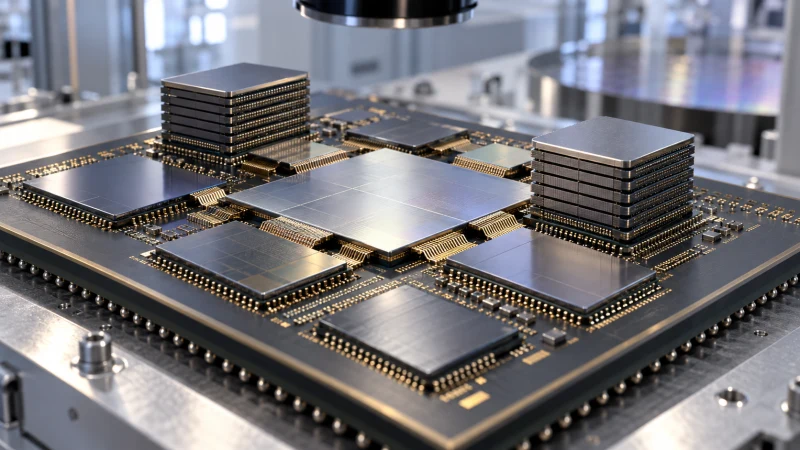
The strongest overlap is in 2.5D integration and panel-level packaging. In both cases, the technical shift is being driven by advanced packaging formats that demand finer patterning, tighter alignment, and new materials. Hybrid bonding is still dominated by foundries at high volume, but it is expected to be a later candidate for migration to OSAT1. Outsourced Semiconductor Assembly and TestA business model in which assembly and test services are provided by a specialized external supplier.2. outsourced assembly and testAn OSAT provider assembles, packages, and tests chips for other companies.s as processes mature and demand outgrows foundry capacity.
The packaging flow is also becoming more lithography-intensive. As interconnect density rises for AIartificial intelligence, HBM1. human body modelESD test model that simulates a person discharging static electricity into a component.2. High Bandwidth MemoryHBM is a stacked DRAM architecture designed to provide very high memory bandwidth., chiplet architectures, and heterogeneous integration, packaging houses are adopting wafer-fab-style patterning methods. Fine-pitch redistribution layers are a key example: RDLRedistribution LayerRDL patterning is a key step in advanced packaging for rerouting chip I/O. fabrication is moving toward more sophisticated lithography to define smaller features than traditional packaging has required.
Intel Foundry described the practical consequences at the interconnect level: fine-pitch bumps raise bump counts sharply versus coarse-pitch schemes, which in turn increases the importance of embedded bridge dies, alignment, and equipment precision. In that environment, the same company can use either foundry-side or packaging-side capabilities depending on the build.
Panel packaging is also changing format. Earlier development lines often targeted large panels around 500 mm per side, while a 310 × 310 mm2 format has gained traction because it is closer to classical 300 mm round process tools. That shift makes it easier for traditional wafer-equipment suppliers to scale for high-performance materials and resolution.
Another area under pressure is hybrid bonding. It remains largely a foundry and IDMintegrated device manufacturerAn IDM makes chips and also controls major parts of the manufacturing flow. technology when volumes are high, but it could move further into OSAT1. Outsourced Semiconductor Assembly and TestA business model in which assembly and test services are provided by a specialized external supplier.2. outsourced assembly and testAn OSAT provider assembles, packages, and tests chips for other companies.s once demand exceeds foundry capacity and the process becomes more standard. That would extend the current pattern seen with 2.5D and panel packaging.
Capacity constraints are a major reason for the shift. Foundries are prioritizing leading-edge silicon, which can push backend and legacy work outward. OSAT1. Outsourced Semiconductor Assembly and TestA business model in which assembly and test services are provided by a specialized external supplier.2. outsourced assembly and testAn OSAT provider assembles, packages, and tests chips for other companies.s are stepping in with processes that are less demanding in resolution but still require advanced-packaging tools, while investment is rising in 2.5D, panel-level, and test equipment. The overall market for advanced packaging is also growing quickly, supporting the capital spending cycle behind this overlap.