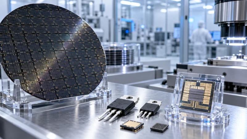
Infineon has successfully processed 300-millimeter silicon carbide wafers into functional power devices at its fab in Villach, Austria. The company says this is the first time such a milestone has been achieved in a full-scale semiconductor fab environment, and that existing silicon manufacturing equipment was used for the work.
The 300 mm format is positioned as a more advanced and more efficient production platform than 200 mm wafers. Infineon states that the larger wafer diameter enables 2.3 times more chips per wafer, which is central to the planned scaling of SiCsilicon carbideSiC is one of the power semiconductor materials being assigned a distinct role in the power delivery chain. manufacturing.
The devices are intended to support applications in automotive, renewable energy, industrial systems and AIartificial intelligence data centers. Infineon highlights traction inverters, on-board chargers, EV chargers, large-scale energy storage, industrial drives and uninterruptible power supplies as established SiCsilicon carbideSiC is one of the power semiconductor materials being assigned a distinct role in the power delivery chain. use cases, while solid-state transformers, circuit breakers and power supply units are emerging roles in AIartificial intelligence data centers.
Infineon also says it has proven the feasibility of its Cold Split technology with 300-millimeter SiCsilicon carbideSiC is one of the power semiconductor materials being assigned a distinct role in the power delivery chain. at its Dresden site. The process separates wafers from a SiCsilicon carbideSiC is one of the power semiconductor materials being assigned a distinct role in the power delivery chain. boule with less material loss and substantially shorter processing time than conventional wire sawing, while reducing capital expenditure by enabling more wafers from the same crystal.
In parallel, the company is continuing its 200-millimeter SiCsilicon carbideSiC is one of the power semiconductor materials being assigned a distinct role in the power delivery chain. manufacturing roadmap and plans the 300-millimeter SiCsilicon carbideSiC is one of the power semiconductor materials being assigned a distinct role in the power delivery chain. technology and ramp timing together with customers and partners. The milestone is presented as part of a broader strategy spanning silicon, silicon carbide and gallium nitride, and Infineon says it will show the first processed 300-millimeter SiCsilicon carbideSiC is one of the power semiconductor materials being assigned a distinct role in the power delivery chain. wafer publicly at electronica in Munich.
The development extends Infineon’s push into wide-bandgap manufacturing and is framed as a step toward secure, future-proof SiCsilicon carbideSiC is one of the power semiconductor materials being assigned a distinct role in the power delivery chain. supply for high-power applications.