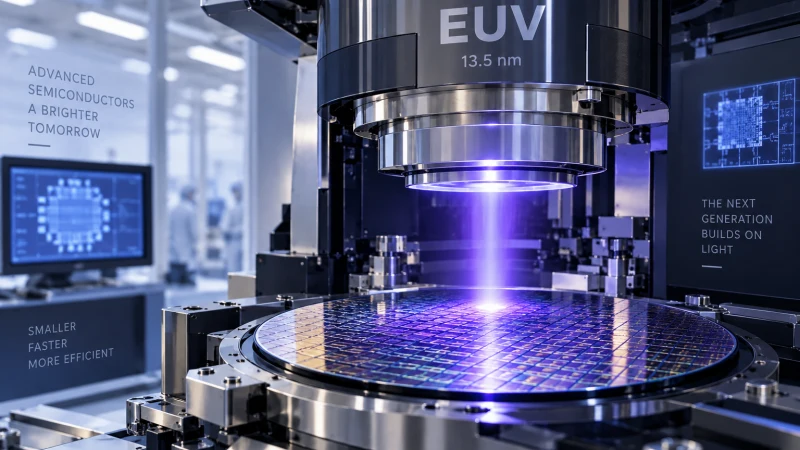
Maskless EUVextreme ultravioletExtremely short-wavelength ultraviolet radiation; EUV lithography uses about 13.5 nm light. lithography is emerging as a proposed alternative to both conventional EUVextreme ultravioletExtremely short-wavelength ultraviolet radiation; EUV lithography uses about 13.5 nm light. scanners and electron-beam direct write. The core idea is to replace the physical photomask with a programmable array or another rapidly addressable optical element, so that circuit patterns can be written directly from digital data onto the wafer.
Conventional EUVextreme ultravioletExtremely short-wavelength ultraviolet radiation; EUV lithography uses about 13.5 nm light. lithography uses 13.5-nanometer light and a reflective optical system to print very small features at high throughput, but every new design still requires an expensive mask set. Maskless EUVextreme ultravioletExtremely short-wavelength ultraviolet radiation; EUV lithography uses about 13.5 nm light. would remove that fixed mask step and shift pattern definition into software-driven exposure. In principle, that would allow a new layout to be loaded from a file rather than fabricated as hardware.
The concept sits between EUVextreme ultravioletExtremely short-wavelength ultraviolet radiation; EUV lithography uses about 13.5 nm light. and electron-beam lithography. E-beam tools are also maskless and can draw extremely fine features, which makes them useful for research, prototyping, and mask production. Their weakness is speed, because electron beams generally write patterns serially, point by point or shape by shape. Multibeam approaches can raise throughput, but they add complexity in beam control, calibration, data handling, and defect management.
A maskless EUVextreme ultravioletExtremely short-wavelength ultraviolet radiation; EUV lithography uses about 13.5 nm light. system could combine the direct digital flexibility of e-beam with the parallel exposure advantage of optical lithography. Millions of controllable elements could expose many features at once, potentially avoiding the serial bottleneck of a single beam. That would shorten iteration cycles, reduce the upfront cost of small production runs, and make advanced prototypes more practical without purchasing a complete mask set.
The technical obstacles remain substantial. EUVextreme ultravioletExtremely short-wavelength ultraviolet radiation; EUV lithography uses about 13.5 nm light. radiation is strongly absorbed by most materials, so the tool must run in vacuum and depend on specialized reflective optics. A programmable pattern generator must survive EUVextreme ultravioletExtremely short-wavelength ultraviolet radiation; EUV lithography uses about 13.5 nm light. exposure, switch with high precision, maintain nanometer-scale placement accuracy, and avoid defects while delivering enough optical power. At very small dimensions, photoresist stochastic effects also become critical, with risks such as rough edges, missing contacts, or unintended bridges. Large pattern files must be processed and delivered in real time as well.
For that reason, the first applications are likely to be selective rather than a replacement for high-volume manufacturing. Maskless EUVextreme ultravioletExtremely short-wavelength ultraviolet radiation; EUV lithography uses about 13.5 nm light. could be used for rapid prototyping, low-volume advanced devices, research, mask repair, or critical layers where flexibility matters more than throughput. In that narrower role, it would complement rather than displace both e-beam and masked EUVextreme ultravioletExtremely short-wavelength ultraviolet radiation; EUV lithography uses about 13.5 nm light..
The broader significance is economic as much as technical: by turning pattern definition from physical infrastructure into software-controlled input, maskless EUVextreme ultravioletExtremely short-wavelength ultraviolet radiation; EUV lithography uses about 13.5 nm light. could reduce the penalty of design changes and open access to advanced lithography for more frequent experimentation and smaller production batches.
Source: SPIESociety of Photo-Optical Instrumentation EngineersThe conference organizer named in the event context. Digital Library.