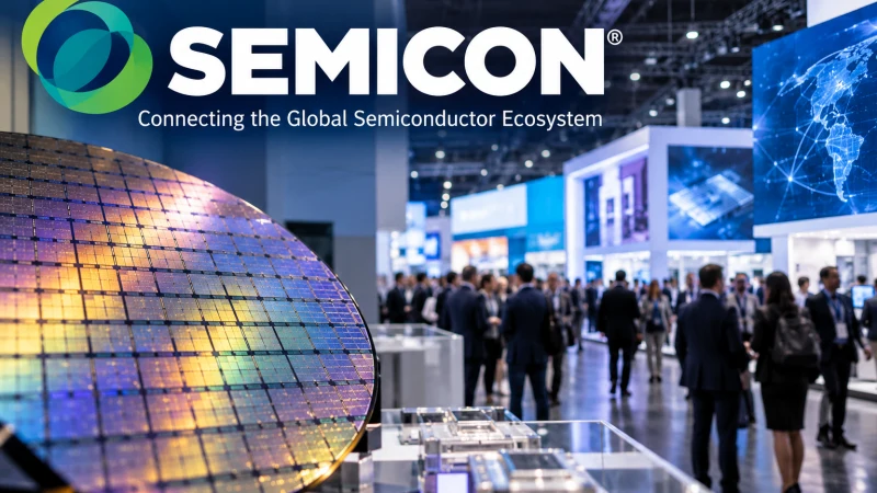
SEMICONSemiconductor ConventionSEMICON is the name of an international trade show for the semiconductor industry organized by SEMI. West 2026 opened in San Francisco with a clear message: semiconductors have reached trillion-dollar scale, and AIartificial intelligence is now shaping the next phase of manufacturing expansion. The event covered lithography, photomasking, wafer inspection, materials, accelerated EDA1. electronic design automationSoftware tools for designing, simulating, verifying and laying out electronic circuits.2. equipment data acquisitionSystem or method for collecting, storing, exchanging or analyzing data., quantum computing, chiplets, and advanced packaging, with autonomous AIartificial intelligence in chip design also featured in a session led by Synopsys CEOchief executive officerCEO identifies the company’s top executive who made the statement. Sassine Ghazi.
One of the most concrete manufacturing announcements came from ZEISS Semiconductor Manufacturing Technology, which introduced two inspection systems as it moved into wafer inspection. Zeiss DUNE measures wafer topography and can correct it individually, targeting wafer bow and helping preserve overlay for later process steps. Zeiss NLX is aimed at 300-mm wafers and is designed to make internal structures in modern packages visible without destroying them, enabling inspection of stacked-die interconnects and early defect detection.
Mitsubishi Chemical Group presented a broader materials push across polymers, films, materials, and chemicals. The company is preparing new materials for semiconductor manufacturing equipment, developing a new biopolymer for PCBprinted circuit boardBoard that mechanically supports components and electrically interconnects them with copper traces.s used in flexible electronics, and working on new materials for formulated silicon in advanced packaging.
Von Ardenne said it is expanding its semiconductor deposition portfolio into panel-level packaging. Its HiPIMShigh-power impulse magnetron sputteringHiPIMS is a physical vapor deposition method used here for barrier and seed layers. approach deposits high-aspect-ratio barrier and seed layers in through-glass via holes, supporting dense, highly adherent functional films and helping transfer established deposition processes from 300-mm wafer formats to larger panel substrates. The company said the approach is intended for advanced packaging applications including through-glass vias and redistribution layers.
Heidenhain introduced a full air-bearing planar platform for demanding step-and-scan applications. The METIS HPhigh purity platform combines direct laser writing and high-resolution optical inspection systems, alongside sub-nanometer motion control and position feedback for wafer manufacturing.
Beyond tools and process technology, workforce development was a major theme. ABMactivity-based managementManagement approach for improving processes based on the activities and their costs., which provides equipment installation, contamination control, and cleanroom services, is preparing workforce solutions after its merger with WGNSTAR. The company pointed to its Technical Training Center in Boise, Idaho, which has capacity for about 500 participants per year in advanced semiconductor manufacturing training.
The event tied together the current priorities of the industry: larger fab infrastructure, tighter inspection and metrology, new materials, and packaging routes that extend beyond the 300-mm wafer. AIartificial intelligence was presented not as a side topic, but as the driver around which manufacturing capacity, tooling, and training are now being organized.