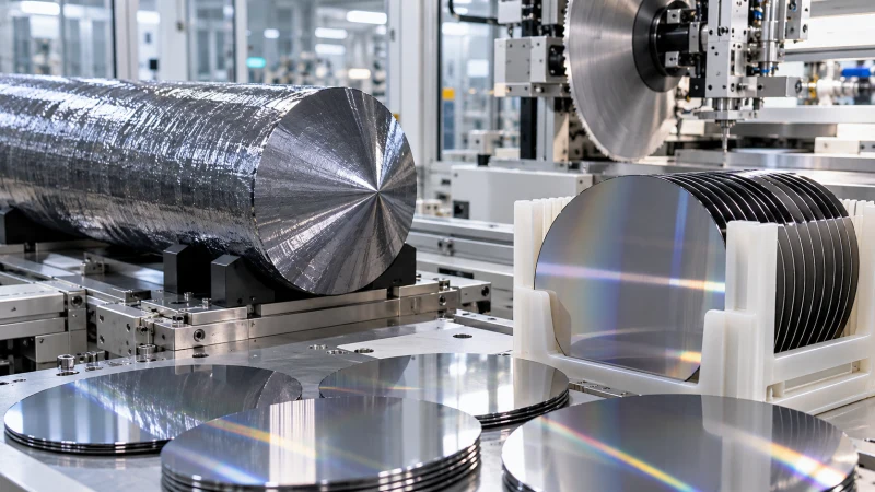
Soitec is pitching the wafer itself as a growing battleground in AIartificial intelligence hardware, with Chief Product Officer René Jonker arguing that the most important performance gains increasingly start in the substrate rather than at the transistor level. His view is that if the right properties are built into the starting material early, foundries do not need to compensate for them later with more complex device engineering.
The company’s business was built around Smart Cut, a process developed after Soitec was spun out of CEA-Leti in 1992. Smart Cut combines ion implantation and wafer bonding to transfer an ultra-thin layer of monocrystalline silicon onto an insulating substrate, creating silicon-on-insulator, or SOI1. silicon on insulatorMaterial or layer used in semiconductor processing, for example for insulation or surface passivation.2. Silicon-On-InsulatorSOI describes a semiconductor structure with an insulating layer beneath the active silicon layer.. Soitec’s early growth came from SOI1. silicon on insulatorMaterial or layer used in semiconductor processing, for example for insulation or surface passivation.2. Silicon-On-InsulatorSOI describes a semiconductor structure with an insulating layer beneath the active silicon layer. supply agreements with AMD and IBMInternational Business MachinesIBM is a US technology company active in computer hardware, software and semiconductor research., while a restructuring in the 2010s pushed the company back to its core and into RF1. radio frequencyHigh-frequency electromagnetic oscillations used, for example, to excite plasmas.2. resonance frequencyQuantity describing a signal’s frequency, bandwidth, spectral behavior or transmission rate.-SOI1. silicon on insulatorMaterial or layer used in semiconductor processing, for example for insulation or surface passivation.2. Silicon-On-InsulatorSOI describes a semiconductor structure with an insulating layer beneath the active silicon layer. for smartphone front-end modules.
Jonker described Soitec as sitting at the bottom of the value chain, where foundries and IDMintegrated device manufacturerAn IDM makes chips and also controls major parts of the manufacturing flow.s such as TSMCTaiwan Semiconductor Manufacturing CompanyTSMC is named as a founding partner of the EPIC Center., GlobalFoundries, STMicroelectronics, Samsung Foundry and UMC buy the wafers as starting material. Fabless companies including Qualcomm, Apple, Broadcom, MediaTek and NXP specify the substrate platforms in their designs, and manufacturing then follows those requirements.
The technical case for engineered substrates is tied to the limits of bulk silicon. Leakage, parasitic capacitance and thermal constraints become harder to manage as scaling continues, while a buried oxide layer under a thin silicon film can address those issues at the material level. In many cases, that approach can reduce power by 30% to 50% without a node shrink.
RF1. radio frequencyHigh-frequency electromagnetic oscillations used, for example, to excite plasmas.2. resonance frequencyQuantity describing a signal’s frequency, bandwidth, spectral behavior or transmission rate.-SOI1. silicon on insulatorMaterial or layer used in semiconductor processing, for example for insulation or surface passivation.2. Silicon-On-InsulatorSOI describes a semiconductor structure with an insulating layer beneath the active silicon layer. remains the company’s best-known platform and is now widely used in RF1. radio frequencyHigh-frequency electromagnetic oscillations used, for example, to excite plasmas.2. resonance frequencyQuantity describing a signal’s frequency, bandwidth, spectral behavior or transmission rate. switches and low-noise amplifiers for 5G phones and Wi-Fi modules. But Soitec now works across five main technology platforms: RF1. radio frequencyHigh-frequency electromagnetic oscillations used, for example, to excite plasmas.2. resonance frequencyQuantity describing a signal’s frequency, bandwidth, spectral behavior or transmission rate.-SOI1. silicon on insulatorMaterial or layer used in semiconductor processing, for example for insulation or surface passivation.2. Silicon-On-InsulatorSOI describes a semiconductor structure with an insulating layer beneath the active silicon layer., FD-SOIFully Depleted Silicon-On-InsulatorA transistor platform that uses a thin buried oxide to improve electrostatic control and reduce power consumption., Power-SOI1. silicon on insulatorMaterial or layer used in semiconductor processing, for example for insulation or surface passivation.2. Silicon-On-InsulatorSOI describes a semiconductor structure with an insulating layer beneath the active silicon layer., Piezoelectric-on-Insulator, and Photonics-SOI1. silicon on insulatorMaterial or layer used in semiconductor processing, for example for insulation or surface passivation.2. Silicon-On-InsulatorSOI describes a semiconductor structure with an insulating layer beneath the active silicon layer.. FD-SOIFully Depleted Silicon-On-InsulatorA transistor platform that uses a thin buried oxide to improve electrostatic control and reduce power consumption. is used for compute units where leakage and power matter, with back-biasing to trade speed against power; Power-SOI1. silicon on insulatorMaterial or layer used in semiconductor processing, for example for insulation or surface passivation.2. Silicon-On-InsulatorSOI describes a semiconductor structure with an insulating layer beneath the active silicon layer. targets high-voltage automotive and industrial circuits; and POI is aimed at acoustic RF1. radio frequencyHigh-frequency electromagnetic oscillations used, for example, to excite plasmas.2. resonance frequencyQuantity describing a signal’s frequency, bandwidth, spectral behavior or transmission rate. filters for 5G and 6G.
Photonics-SOI1. silicon on insulatorMaterial or layer used in semiconductor processing, for example for insulation or surface passivation.2. Silicon-On-InsulatorSOI describes a semiconductor structure with an insulating layer beneath the active silicon layer. has become especially important in AIartificial intelligence infrastructure. As electrical interconnects run into bandwidth limits, traffic shifts toward fiber, and photonics moves into the interface where electrons are converted into photons. Soitec sees this platform as a key enabler for optical waveguides in silicon-based infrastructure and for co-packaged optics in AIartificial intelligence data centers.
The company is also extending its materials strategy beyond silicon. SmartSiC reuses a single-crystal silicon carbide donor wafer multiple times and bonds a thin layer onto a conductive base to lower the cost of SiCsilicon carbideSiC is one of the power semiconductor materials being assigned a distinct role in the power delivery chain. power devices for EV inverters. RF1. radio frequencyHigh-frequency electromagnetic oscillations used, for example, to excite plasmas.2. resonance frequencyQuantity describing a signal’s frequency, bandwidth, spectral behavior or transmission rate.-GaNgallium nitrideGaN is another material platform mentioned for use in different power delivery roles. on insulator is being developed for 6G power amplifiers and aerospace, while FD-SOIFully Depleted Silicon-On-InsulatorA transistor platform that uses a thin buried oxide to improve electrostatic control and reduce power consumption. is being pushed to smaller geometries for energy-conscious on-device AIartificial intelligence in phones and wearables.
Jonker framed the next competitive phase as a shift toward heterogeneous materials, with gallium nitride and silicon carbide joining silicon in more specialized applications. In his view, substrates win not by raw physics alone but by adding new functionality at the cheapest point in the manufacturing flow, where they can influence the rest of the stack from the outset.