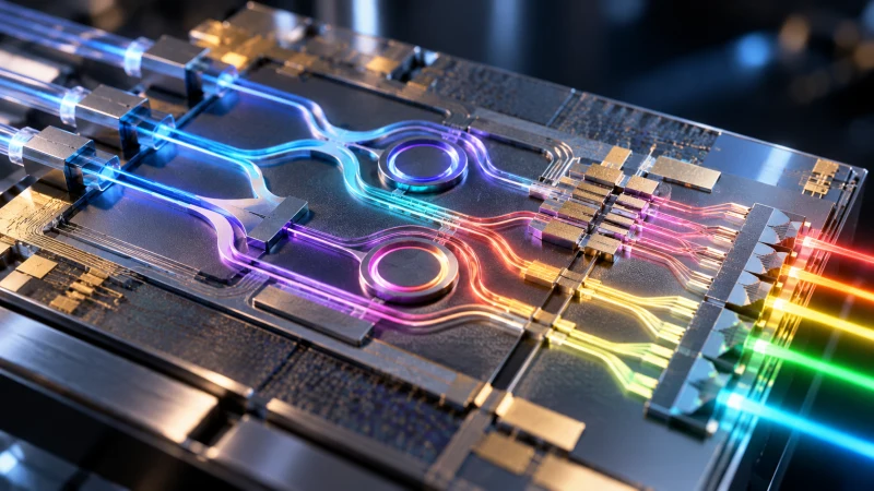
Silicon photonics is moving from development labs toward high-volume manufacturing as AIartificial intelligence and HPC1. High Performance ComputingCompute applications with particularly high performance demands, cited here as a driver for packaging and testing.2. high-performance computingHPC denotes compute-intensive chips that require advanced testing support. workloads push data-center links beyond the limits of conventional electrical interconnects in power, latency, and reach. Near-packaged optics and co-packaged optics are part of that shift, but the main challenge is no longer only photonic device performance. The test infrastructure has to evolve as well.
Unlike electrical test, optical test depends on precise fiber alignment and stable coupling into and out of very small structures. Small changes in fiber position or angle can alter insertion loss and measured performance enough to blur the line between true device variation and test-induced variation. That makes repeatable optical connection a core manufacturing requirement rather than a laboratory convenience.
High-volume workflows therefore need automated alignment that can locate the optical interface quickly and optimize coupling. The process may use image-based positioning, area scans, and gradient-search feedback loops to achieve active alignment. In practice, this can mean optimizing six degrees of freedom: X, Y, and Z plus three rotational axes. Multi-channel interfaces add another layer of complexity, because alignment must produce consistent coupling across channels, not just peak performance on one path.
Polarization is another production variable. Photonic structures can respond differently depending on the polarization state of incoming light, so polarization has to be measured and controlled as part of a repeatable test flow. The result is a measurement process that combines alignment, optimization, and characterization instead of a simple mechanical setup step.
Beyond optical setup, a photonic integrated circuit may still require conventional electrical characterization alongside optical measurements. Typical checks include insertion loss, channel-to-channel uniformity, optical attenuation, photodetector responsivity, and wavelength-dependent behavior. To keep test time under control, electrical and optical operations should run in parallel wherever possible rather than strictly one after another.
The same parallelism applies to instrumentation. High-volume environments benefit from integrated control of lasers, power meters, and other optical tools, along with automated calibration and compensation as the test cell grows more complex. Advantest’s work in this area includes support for multiple optical instruments and parallel power-meter operation within one test environment.
Scaling photonics test also requires collaboration across the ecosystem. A complete solution spans automated test equipment, wafer probing, optical positioning, fiber interfaces, instrumentation, device design, and manufacturing processes. Advantest and FormFactor have worked together on a wafer-level photonics test environment that combines electrical test, wafer handling, optical instruments, and automated fiber alignment. The broader issue is integrating these elements into a repeatable production workflow that can support silicon photonics, NPO, and CPOco-packaged opticsOptical devices and CPUs are integrated into a single package at commercial scale.
The transition to high-volume photonic production will depend on test systems that can coordinate optical alignment, electrical and optical measurement, automation, and interoperability as one manufacturing problem. Device advances alone are not enough if the test flow cannot deliver the required repeatability, throughput, and economics.