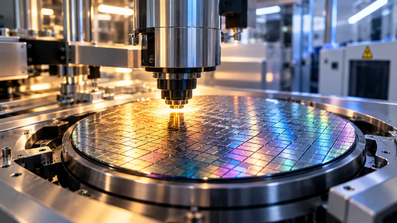
Samsung Electronics and ASMLAdvanced Semiconductor Materials LithographyASML is the lithography equipment maker named in the report. have expanded their long-standing partnership with a stronger focus on High-NAnumerical apertureOptical measure of the light-gathering angle of a lens, related to resolution. EUVextreme ultravioletExtremely short-wavelength ultraviolet radiation; EUV lithography uses about 13.5 nm light. lithography and advanced semiconductor manufacturing. The companies say the work is intended to support the performance and efficiency demands of future chip production, with Samsung highlighting a planned role in the next generation of lithography infrastructure.
A central part of the announcement is Samsung’s entry into an industry initiative to advance a new 12-inch photomask platform for High-NAnumerical apertureOptical measure of the light-gathering angle of a lens, related to resolution. EUVextreme ultravioletExtremely short-wavelength ultraviolet radiation; EUV lithography uses about 13.5 nm light.. The industry has relied on 6-inch photomask formats for decades. According to the companies, moving to larger masks should raise fab productivity, lower chipmaking costs and remove stitching constraints, which become more relevant as patterning requirements tighten.
Samsung says it will work with industry partners on the required mask technologies and supporting infrastructure. The company points to its experience in both memory and foundry manufacturing, as well as its background in advanced EUVextreme ultravioletExtremely short-wavelength ultraviolet radiation; EUV lithography uses about 13.5 nm light. lithography, as the basis for taking part in the transition to the larger mask format.
In parallel, Samsung plans to introduce ASMLAdvanced Semiconductor Materials LithographyASML is the lithography equipment maker named in the report.’s High-NAnumerical apertureOptical measure of the light-gathering angle of a lens, related to resolution. extreme ultraviolet lithography into future DRAM1. dynamic random access memoryMemory technology or system for temporarily or permanently storing digital information.2. dynamic random-access memoryDRAM is a volatile memory technology high-volume manufacturing by 2028, which it says would be the first such deployment in the industry. Samsung describes the move as a way to extend the DRAM1. dynamic random access memoryMemory technology or system for temporarily or permanently storing digital information.2. dynamic random-access memoryDRAM is a volatile memory technology scaling roadmap, with improved resolution enabling process simplification and higher efficiency. The companies frame the collaboration as an ongoing effort to develop technologies for advanced memory and logic manufacturing.