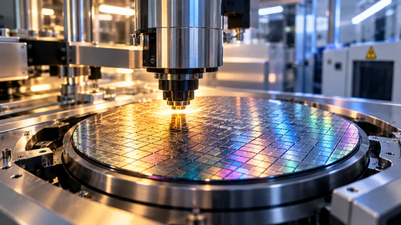
Test cost is becoming a central issue for co-packaged optics as optical component testing approaches, and in some cases may exceed, the cost of manufacturing the device itself. The debate is no longer about whether CPOco-packaged opticsOptical devices and CPUs are integrated into a single package works; the immediate challenge is how to diagnose failures, screen parts earlier, and scale the flow toward high-volume manufacturing without letting a low-cost optical engine jeopardize a very expensive ASICapplication-specific integrated circuitIntegrated circuit customized for a specific task or GPUgraphics processing unitA GPU is a parallel graphics processor widely used for AI acceleration..
A major technical problem is failure localization. Engineers must define reference planes and boundaries across the electrical, physical, and optical interfaces, then de-embed everything inserted between them, such as probes, sockets, traces, connectors, and patch cords. The same boundary conditions have to be maintained across multiple test insertions so the root cause can be isolated more reliably. In practice, that can mean emulating the missing half of a system with a known-characterized substitute or using a golden reference laser source.
Loopback testing and monitor photodiodes are emerging as practical tools for diagnosis. Customers are adding photodiodes into the light path so unexpected transmit- or receive-path behavior can be traced back. Others want tap capability to route signals to characterization equipment or simply monitor power during loopback or mission-mode testing. That improves observability, but it also exposes a trade-off: if a failure occurs and bit-error-rate targets are missed, the source of the problem may remain unclear without additional tap points or instrumentation.
The distinction between near-packaged optics and co-packaged optics matters, but not always in the way the labels suggest. Some NPO implementations allow optical engines to be detached, which can simplify isolation. Even so, rework and reattachment farther downstream are described as painful enough that customers still want known-good optical engines. In more integrated CPOco-packaged opticsOptical devices and CPUs are integrated into a single package systems, decoupling the package elements becomes even more important, and design-for-test becomes a way to correlate measurements on individual pieces with failures at package level.
Retimed NPO and linear-drive NPO behave very differently in test. A retimed NPO carries its own DSP1. differential signal processingSignal processing based on differences between two signals, often rejecting common interference.2. digital signal processing, so the optical engine can be compliance-tested on its own much like a pluggable module. A linear-drive NPO removes the DSP1. differential signal processingSignal processing based on differences between two signals, often rejecting common interference.2. digital signal processing, leaving the host ASICapplication-specific integrated circuitIntegrated circuit customized for a specific task SerDes1. Serializer/DeserializerSerDes is the high-speed I/O block that receives, conditions, and retransmits the signal.2. Serializer-DeserializerSerDes converts parallel signals into serial data streams and back. to drive the optics through linear drivers and TIAs, which makes the electrical and optical paths effectively one signal chain. In that case, a failed link cannot easily be assigned to one side or the other, and the test problem looks much closer to CPOco-packaged opticsOptical devices and CPUs are integrated into a single package. Thermal behavior is another issue, especially because the optical parts dissipate significant power and the electrical reach is shorter in CPOco-packaged opticsOptical devices and CPUs are integrated into a single package.
The economics are changing just as sharply. With optical engines integrated around AIartificial intelligence accelerators and network-switch devices valued at roughly $40,000 to $50,000, the industry is moving toward more aggressive early testing to protect the expensive chip in the middle of the package. That shifts attention toward pre-assembly screening, additional wafer-level or optical-engine-level test, and more engineering controls before packaging. Yield learning then becomes the payoff as production scales.
For high-volume manufacturing, the ecosystem still needs to mature. Additional screening, burn-in, more insertions, and stronger process controls are seen as near-term measures while standards and multi-source manufacturing catch up. Industry groups are also trying to align on the optical power, bias conditions, and other criteria needed for scalable manufacturing. The discussion also highlights an organizational split inside many companies: photonics teams and semiconductor high-volume test teams have to reconcile optical performance, uptime, software support, serviceability, and modular test-cell design before CPOco-packaged opticsOptical devices and CPUs are integrated into a single package can move smoothly into volume production.
Across the discussion, the same conclusion emerges: optical test is becoming too expensive and too important to treat as an afterthought. The cost of testing an optical component is moving toward the cost of making it, and the pressure to know that the die and the optical engine are good before final integration is now shaping both test architecture and manufacturing strategy.