Short updates from the semiconductor industry, with context and links to the relevant chapters.

October 30, 2026
Industry & People
HBM and DRAM supply remains tight across the industry, while advanced packaging capacity is being pushed harder by AI demand. At the same time, foundries, equipment makers and AI infrastructure suppliers are expanding investments, pricing, and partnerships to keep pace with next-generation compute and memory ramps.
Read more →
·
Advanced Packaging
October 29, 2026
Industry & People
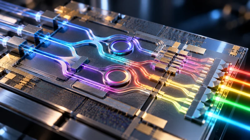
AI systems can still stall even with tens of thousands of GPUs when data movement becomes the bottleneck. Silicon photonics and co-packaged optics (CPO) are emerging as ways to move more of that traffic from electrical links to light, reducing loss, power consumption, and heat in large-scale AI networks.
Read more →
·
How Does It Work?
October 22, 2026
Industry & People
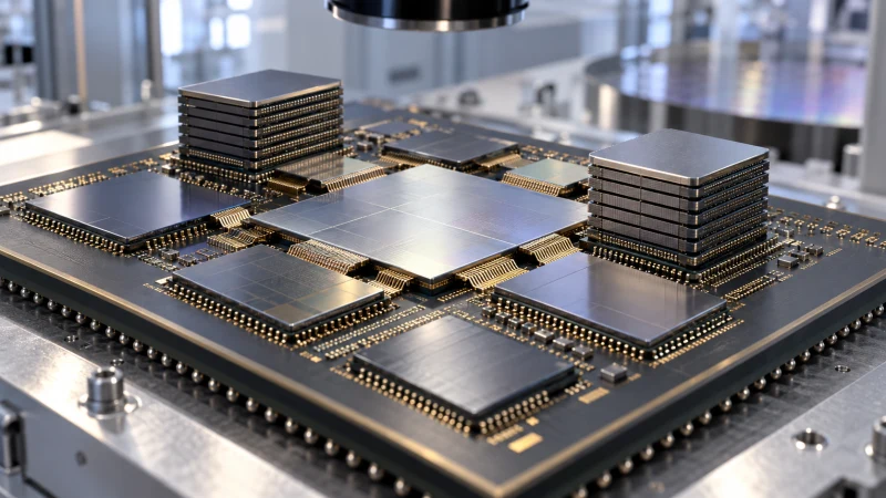
Advanced packaging is pushing foundries and OSATs into each other’s territory. The overlap is strongest in 2.5D integration and panel-level assembly, where lithography-like materials, finer RDL features, and new equipment are moving into packaging lines. Hybrid bonding remains mostly a foundry activity for now, but it is already being positioned as a future spillover area as capacity tightens.
Read more →
·
Advanced Packaging
October 20, 2026
Industry & People
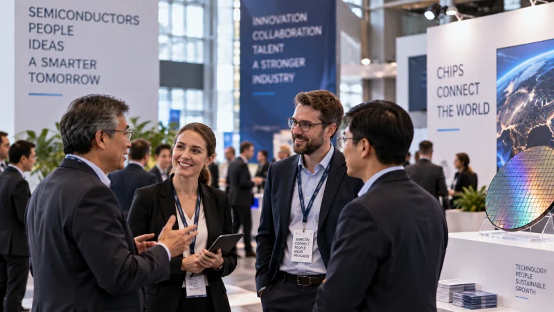
Singapore is tying together chip research, startups, and manufacturing with platforms for SiC power devices, metalenses, and silicon photonics. A*STAR, MetaOptics, Advanced Micro Foundry, and GlobalFoundries illustrate how deep-tech work can move from laboratory development into industrial-scale production.
Read more →
·
How Does It Work?
October 20, 2026
Industry & People
Artificial intelligence is shifting the semiconductor bottleneck from individual devices to the full computing system. Applied Materials says future progress will depend on tighter coordination across processors, memory, interconnects, advanced packaging, power efficiency and thermal management, with earlier collaboration needed to avoid late-stage integration problems.
Read more →
·
Advanced Packaging
October 16, 2026
Industry & People
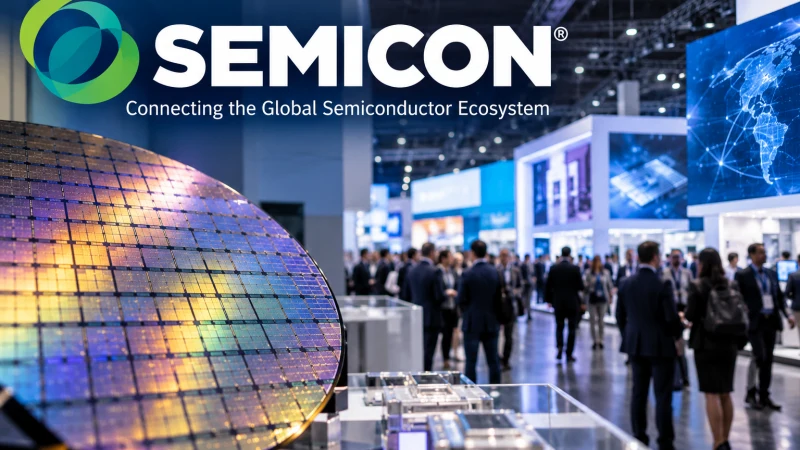
SEMICON West 2026 in San Francisco framed semiconductors as a trillion-dollar industry and put AI at the center of the next fab buildout. The show highlighted new inspection tools from ZEISS, panel-level packaging deposition from Von Ardenne, motion-control equipment from Heidenhain, materials work from Mitsubishi Chemical Group, and workforce programs led by ABM.
Read more →
·
Wafer Fabrication
October 16, 2026
Industry & People
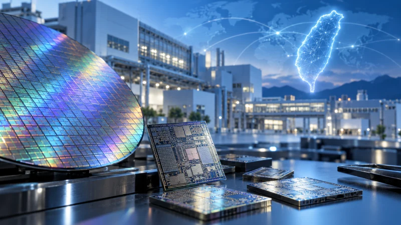
At iTechCon 2026, industry and research speakers argued that AI value is shifting from standalone chips toward co-design across hardware, models, software, packaging, and system architecture. The discussion highlighted Taiwan’s strengths in semiconductor manufacturing and advanced packaging, but also its need to deepen software capability, cross-disciplinary talent, and startup support as AI moves into inference, agentic AI, edge devices, and physical AI.
Read more →
·
How Does It Work?
October 16, 2026
Industry & People
A dense week in semiconductors brought fresh fab expansion, new packaging and test initiatives, stronger AI-related spending signals, and continued momentum in China’s memory and EUV efforts. TSMC and ASML both reported strong quarters, while startups in photonics and 3D compute secured new funding and quantum hardware teams posted notable technical progress.
Read more →
October 14, 2026
Industry & People
At Ayar Labs’ CPO Summit, Meta, Broadcom, AMD, MediaTek, Lumentum, Wiwynn and Upscale AI focused on whether the optical interconnect ecosystem can be ready for a 2028 demand surge. The discussions centered on manufacturability, supply-chain scale, interoperability and the OCI MSA as co-packaged optics moves toward high-volume deployment.
Read more →
·
Optoelectronics & Photonics
October 14, 2026
Industry & People
ASM International is highlighting how the move toward more complex 3D devices is shifting attention beyond lithography and onto the materials and process steps needed to build them reliably.
Read more →
·
How does it work?
October 8, 2026
Industry & People
Test vendors are adapting their production tools for near-packaged and co-packaged optics as data center deployments move toward higher volume. The main pressure points are optical alignment, connector uncertainty, thermal load, and the lack of optical design-for-testability in today’s flows.
Read more →
·
Optoelectronics & Photonics
October 6, 2026
Industry & People
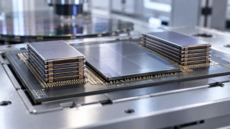
South Korean memory makers are reportedly quoting much higher long-term contract prices for sixth-generation high-bandwidth memory. HBM4 is expected to sell for about US$500 to US$550 in 2026, while 2027 quotes could reach US$1,400 to US$1,600, reflecting a 1.8x to 1.9x increase.
Read more →
·
Fundamentals
September 30, 2026
Industry & People
HBM is becoming a major cost driver in GPU-based CoWoS packaging, raising the question of whether memory can still be treated as a passive part of AI computing. The discussion ties back to the long-running memory wall that has influenced semiconductor development for decades.
Read more →
·
Advanced Packaging
September 30, 2026
Industry & People
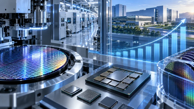
Global Foundry 2.0 market revenue climbed to a record $96.6 billion in the second quarter of 2026, driven by data-center expansion and stronger demand across networking, power management, mature-node chips, packaging, and test.
Read more →
·
Wafer Fabrication
September 30, 2026
Industry & People
At A*STAR’s Innovate Together 2026, industry specialists discussed how AI is reshaping packaging requirements, from hybrid bonding and optical interconnects to tighter process control.
Read more →
·
Advanced Packaging