Short updates from the semiconductor industry, with context and links to the relevant chapters.
October 30, 2026
Manufacturing & Processes
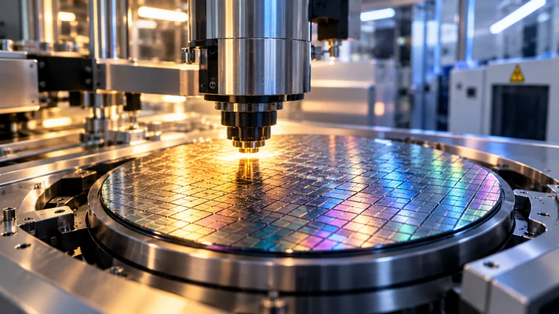
AI is reshaping semiconductor factories as much as the systems they produce. Intel Foundry says scaling AI now depends not only on smaller transistors, but also on power delivery, connectivity, advanced packaging and supply chain resilience, while AI is also being used to improve quality and shorten yield learning in manufacturing.
Read more →
·
How does it work?
October 26, 2026
Manufacturing & Processes
As co-packaged optics moves toward high-volume manufacturing, test strategies are shifting toward earlier screening, known-good optical engines, and tighter failure isolation. The discussion centers on how to keep expensive GPUs and ASICs from being taken down by a faulty photonics device while controlling the rising cost and complexity of optical test.
Read more →
·
Advanced Packaging
October 26, 2026
Manufacturing & Processes
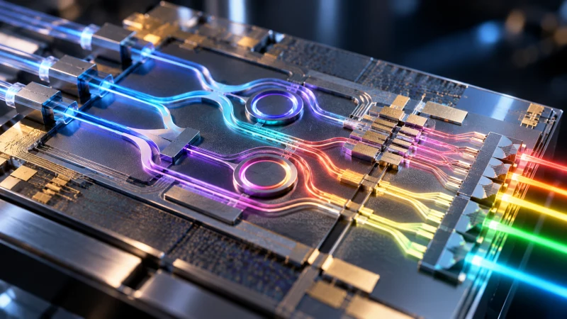
As silicon photonics moves toward production-scale deployment in data centers, test flows are becoming a central manufacturing problem. Automated optical alignment, polarization control, combined electrical and optical measurements, and integrated instrumentation are all needed to keep throughput and repeatability at HVM levels.
Read more →
·
How does it work?
October 22, 2026
Manufacturing & Processes
SEMICON West 2026 highlighted smart manufacturing themes such as digital twins, agentic AI and physical AI, while PDF Solutions prepared demonstrations of Exensio Aurora for semiconductor manufacturing and supply-chain analytics. The central issue is no longer whether AI can surface useful recommendations, but how fabs define when those recommendations may become authorized actions, who approves them, and how each escalation is documented.
Read more →
·
How does it work?
October 22, 2026
Manufacturing & Processes
Multi-chip and stacked-die designs are becoming a main route for continued scaling in AI and HPC, but they also raise current density, multiply voltage domains, and tighten power-delivery constraints inside the package. Intel Foundry is advancing integrated voltage-regulation options, including FIVR, CoaxMIL magnetic inductors, and the capacitor-based C2VR approach, to move conversion closer to the load and improve power integrity.
Read more →
·
Advanced Packaging
October 21, 2026
Manufacturing & Processes
As five semiconductor plants in India enter commercial production, OSATs are under pressure to secure enough test capacity for a wider mix of devices. NI says Kaynes Semicon has chosen its Semiconductor Test System, while other Indian OSATs are still qualifying equipment and evaluating test architectures for both legacy parts and new designs.
Read more →
·
Wafer Fabrication
October 21, 2026
Manufacturing & Processes
High-volume testing for co-packaged optics is being pushed beyond single-die operation, but fiber alignment remains the main bottleneck. At the same time, connector durability, warpage, and the need to combine optical and electrical measurements are making production test architectures more complex.
Read more →
·
Optoelectronics & Photonics
October 8, 2026
Manufacturing & Processes
Advanced process control is moving closer to the tool, but the sensor data needed for in-situ AI/ML analysis is growing faster than fabs can easily absorb. Streaming traces, higher sampling rates and broader equipment parameter sets are pushing fabs to balance faster yield learning against the loss of process context.
Read more →
·
Fundamentals
September 28, 2026
Manufacturing & Processes
Advanced substrates are moving away from interchangeable standard parts as larger packages, finer routing, and embedded functions tighten the link between material set, layout, and process window. Capacity still matters, but it no longer solves the full manufacturing problem by itself.
Read more →
·
Advanced Packaging
September 22, 2026
Manufacturing & Processes
As AI accelerators and HPC processors scale to more cores, chiplets, and scan elements, Synopsys is pairing unified test compression with a programmable streaming fabric to move test data more efficiently across large hierarchical designs.
Read more →
·
Fundamentals
September 17, 2026
Manufacturing & Processes
onsemi has introduced an Embedded Power Platform that uses the silicon wafer itself as the package foundation, embedding multiple dies and combining electrical, thermal, and mechanical co-design to raise power density in AI and automotive power systems.
Read more →
·
Advanced Packaging
September 8, 2026
Manufacturing & Processes
Samsung Electronics is joining an industry initiative for a new 12-inch photomask platform and plans to introduce ASML’s High-NA EUV lithography into future DRAM high-volume manufacturing by 2028.
Read more →
·
Photolithography
August 27, 2026
Manufacturing & Processes
As HBM stacks grow taller, DRAM makers are facing a sharper mix of die thinning, TSV area loss, heat removal problems and tighter manufacturing capacity, with yield increasingly at risk.
Read more →
·
How does it work?
August 24, 2026
Manufacturing & Processes
Emerson argues that chip validation is no longer a final checkpoint, but a core part of engineering as chiplets and heterogeneous integration push traditional end-of-line test methods to their limits. The proposed answer is a more connected test infrastructure, paired with AI-based analysis of the resulting data.
Read more →
·
Fundamentals