Short updates from the semiconductor industry, with context and links to the relevant chapters.
November 1, 2026
Research
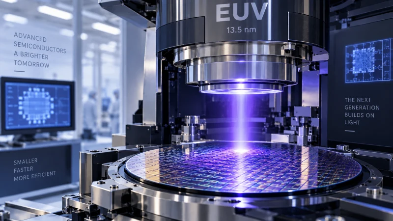
Intel is already using High-NA EUV on selected layers in a subset of Panther Lake processors, Samsung has outlined a DRAM rollout for 2028, and TSMC plans advanced-node volume adoption from 2030. The technology still faces smaller exposure fields, stitching constraints and tough economics, but recent production milestones suggest its deployment curve is only delayed, not derailed.
Read more →
·
Photolithography

October 30, 2026
Research
AI is already becoming effective in semiconductor design, where models, rules, constraints, and solver outputs define a structured environment. Manufacturing is harder because it has to manage the physical reality of as-built geometry, process drift, material variation, and measurement evidence across the package and process flow.
Read more →
·
Advanced Packaging
October 29, 2026
Research
AI agents and digital twins are pushing design decisions earlier in the chip flow, but verification, trust in surrogate models, and multi-physics complexity remain major limits. Several experts argue that the next phase of shift left will be less about freezing specifications early and more about refining architectures and implementation choices as new information appears.
Read more →
·
How does it work?
October 29, 2026
Research
Rising AI performance targets are putting semiconductor manufacturing materials, process equipment, and advanced packaging under new pressure. The focus is shifting from chip design alone to the entire production chain, where tighter tolerances, stronger thermal demands, and more complex multi-die packages now determine whether advanced designs can be built reliably at scale.
Read more →
·
How does it work?
October 27, 2026
Research
Exploding bandwidth demand from cloud and AI workloads is pushing optical links closer to silicon, from pluggable transceivers to co-packaged optics and eventually 3D integrated optical fabrics. imec highlights a roadmap built around higher per-lane rates, denser packaging, and heterogeneous electro-optic materials such as lithium niobate, lithium tantalate, and barium titanate.
Read more →
·
Optoelectronics & Photonics
October 26, 2026
Research
A new industry push is aligning photomask makers, equipment suppliers, and chipmakers around a 12-inch mask format by 2031, driven by a productivity case tied to High-NA EUV. The panel discussion also pointed to growing demand for new mask-etch capability, curvilinear masks, and better supply-chain coordination.
Read more →
·
Photolithography
October 26, 2026
Research
Accellera Systems Initiative has approved Functional Safety Language Standard 1.0, a data model and syntax for moving functional safety information more reliably between tools, engineering teams, and companies. The standard is aimed at a long-standing problem in semiconductor development: keeping assumptions, failure analyses, and verification results aligned as safety data moves from IP to chips and into system integration.
Read more →
October 25, 2026
Research
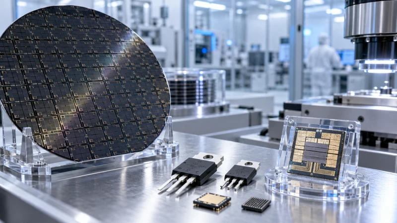
Mivium is positioning itself as a source-material company for gallium nitride, producing phase-pure, submicron GaN powder in Fremont, California and backing it with independent characterization. The company says the same platform can also extend to gallium oxide and boron nitride, while initial GaN deposition work has already started in-house.
Read more →
·
How It Works
October 22, 2026
Research
Traditional Process, Voltage and Temperature characterization is no longer enough to describe how modern processors behave under real operating conditions. A workload-aware extension, PVTW, adds a fourth axis: the specific compute, memory or I/O stress applied to the device while voltage and frequency margins are swept.
Read more →
·
How It Works

October 22, 2026
Research
A proposed self-aligned complementary FET architecture stacks NMOS and PMOS devices vertically to push density past the limits of conventional GAA nanosheets. Digital twin simulation shows a 6T SRAM bit cell of 0.0094 µm², a 52.7% area reduction versus N3, and at least a 10 nm overlay window on critical contact layers.
Read more →
·
Fundamentals
October 22, 2026
Research
At SPIE Photomask Technology + Extreme Ultraviolet Lithography, an expert panel argued that edge placement error is no longer just a lithography metric. The discussion tied EPE to mask structure, scanner behavior, resist variability, etch, metrology, OPC, and downstream integration, and called for richer measurements, explainable AI, and cross-domain workflows to improve manufacturability and yield.
Read more →
·
Fundamentals
October 20, 2026
Research
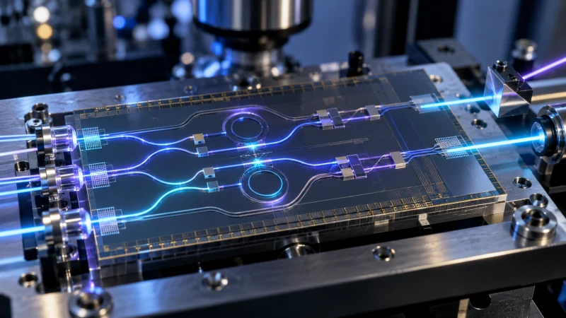
ASML and Xanadu are examining whether tighter lithographic control can reduce photon loss in photonic quantum processors. The work ties optical loss to line-edge roughness, sidewall profile, process variability and pattern-transfer effects, with the goal of improving the prospects for fault-tolerant photonic hardware.
Read more →
·
Photolithography
October 19, 2026
Research
Embedded memory has become the main limiter in AI and HPC SoCs, taking more than half of total die area while constraining bandwidth, latency, and energy efficiency. Synopsys is addressing that shift with memory IP tuned for RibbonFET and PowerVia, backed by SRAM and Register File silicon results on Intel 18A that show 5% to 10% density gains and up to about 4% ISO-power performance improvement.
Read more →
·
Wafer Fabrication
October 19, 2026
Research
Researchers from UC Berkeley, Samsung Electronics, and Intel have reported a nanoelectromechanically gated gain-cell eDRAM design that addresses three long-standing drawbacks of gain-cell memory: limited retention, parasitic coupling, and boosted write-voltage requirements. The approach targets the density and energy-efficiency advantages of gain cells while trying to remove the mechanisms that have kept embedded DRAM from scaling more cleanly.
Read more →
·
Devices
October 18, 2026
Research
Maskless EUV lithography could offer a middle ground between serial electron-beam writing and conventional masked EUV. Instead of relying on a custom photomask, a programmable optical element would project digital patterns directly onto the wafer, with the aim of reducing mask cost and shortening design iteration cycles for low-volume and rapidly changing chip designs.
Read more →
·
Photolithography