Short updates from the semiconductor industry, with context and links to the relevant chapters.

October 5, 2026
Research
Researchers from HUST, Hong Kong Polytechnic University, UC Santa Barbara, and the National University of Singapore report ballistic p-type WSe2 monolayer transistors with lower contact resistance and higher on-state current. The work targets one of the main bottlenecks for extending 2D semiconductors toward sub-1-nm CMOS circuits.
Read more →
·
Devices
October 5, 2026
Research
Researchers at the University of California, Santa Cruz have explored backside clock meshes for 2 nm GAAFET BSPDN technology. The approach uses the backside metal stack to reduce clock skew and save routing resources on premium frontside layers, while still relying on through-silicon vias to reach flip-flops on the frontside.
Read more →
·
How Does It Work?
October 5, 2026
Research
Researchers from Syracuse University, Friedrich-Alexander-Universität Erlangen-Nürnberg, and TU Dresden have introduced RAPID, a row-parallel arithmetic processing-in-DRAM architecture. The approach adds migration cells for local horizontal movement between neighboring bitlines and inversion cells for in-array logical inversion, allowing DRAM to work on row-parallel, bit-parallel data instead of forcing column-oriented, bit-serial reorganization.
Read more →
·
How does it work?
October 2, 2026
Research
A free webinar will examine how full-wave finite-element simulation and semianalytical multipole decomposition in COMSOL Multiphysics can be used to design dielectric metasurfaces that control transmission, reflection, and absorption. The focus is on silicon and gallium nitride structures, where different multipole mechanisms are arranged to produce anomalous absorption enhancement and q-BIC-related spectral shaping.
Read more →
·
Optoelectronics & Photonics

October 1, 2026
Companies & Market
Renesas Electronics has introduced a dual-side-cooled 650-V GaN device for high-voltage power conversion in AI data centers. The new package spreads heat from both the top and bottom, cuts footprint by 57% versus the prior TOLT option, and targets 800-V intermediate bus converters in space- and thermally constrained racks.
Read more →
·
How it works
October 1, 2026
Companies & Market
Applied Materials and Besi are widening their joint development work on advanced packaging by bringing Besi into Applied’s EPIC Center as an Innovation Partner. The collaboration now reaches beyond hybrid bonding into next-generation interconnect architectures, 3D IC scaling, logic and memory integration, and photonics-oriented applications.
Read more →
·
Advanced Packaging

September 30, 2026
Industry & People
HBM is becoming a major cost driver in GPU-based CoWoS packaging, raising the question of whether memory can still be treated as a passive part of AI computing. The discussion ties back to the long-running memory wall that has influenced semiconductor development for decades.
Read more →
·
Advanced Packaging

September 30, 2026
Supply Chain & Sites
India’s push to build a domestic chip ecosystem is already pulling the materials supply chain onshore. As Tata Electronics advances its Dholera fab and packaging projects take shape in Sanand, suppliers of industrial gases, wet chemicals and photoresists are positioning themselves near future customers in Gujarat.
Read more →
·
Wafer Fabrication

September 30, 2026
Industry & People
Global Foundry 2.0 market revenue climbed to a record $96.6 billion in the second quarter of 2026, driven by data-center expansion and stronger demand across networking, power management, mature-node chips, packaging, and test.
Read more →
·
Wafer Fabrication
September 30, 2026
Industry & People
At A*STAR’s Innovate Together 2026, industry specialists discussed how AI is reshaping packaging requirements, from hybrid bonding and optical interconnects to tighter process control.
Read more →
·
Advanced Packaging
September 30, 2026
Research
China’s 3D DRAM effort is shifting beyond lab work, with IMECAS, SAMT, CXMT and NAURA Technology Group all involved in the move toward wafer processes and equipment. The development signals progress from early research, but mass production still faces major technical hurdles.
Read more →
·
Wafer Fabrication
September 29, 2026
Design & EDA
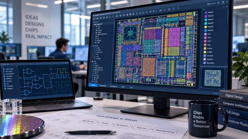
Siemens and TSMC are broadening their collaboration on design tools with an emphasis on AI-assisted workflows, advanced packaging, and support for newer manufacturing processes. The announcement highlights an AI agent meant to identify and correct design rule violations before they block a layout from moving forward.
Read more →
September 29, 2026
Companies & Market
Infineon will supply silicon carbide power devices for Eaton’s medium-voltage solid-state transformer platform, aiming to improve efficiency, power density, and reliability in AI data center power conversion.
Read more →
·
Devices
September 29, 2026
Companies & Market
Applied Materials has brought KIOXIA into its EPIC Center ecosystem to co-develop advanced memory-cell structures, multi-chip stacking architectures and materials engineering approaches aimed at higher density, bandwidth and energy efficiency for AI-focused memory systems.
Read more →
·
Advanced Packaging
September 29, 2026
Design & EDA
As more computing power is concentrated in a single system, the bottleneck is shifting from individual die performance to the complexity of connecting multiple chips, memory stacks, power delivery, and sometimes optical components inside one compact package.
Read more →
·
Advanced Packaging