Short updates from the semiconductor industry, with context and links to the relevant chapters.
October 8, 2026
Manufacturing & Processes
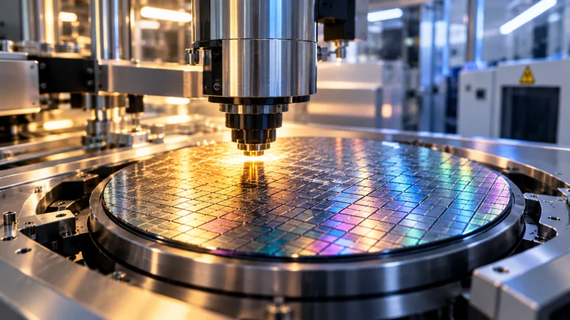
Advanced process control is moving closer to the tool, but the sensor data needed for in-situ AI/ML analysis is growing faster than fabs can easily absorb. Streaming traces, higher sampling rates and broader equipment parameter sets are pushing fabs to balance faster yield learning against the loss of process context.
Read more →
·
Fundamentals
October 8, 2026
Companies & Market
GlobalFoundries will add manufacturing capacity in Malta, New York, to supply silicon interposers for TSMC’s CoWoS advanced packaging ecosystem. The multi-year agreement is aimed at expanding the U.S. base for AI and high-performance computing packaging and is expected to support volume ramp-up from the first half of 2028.
Read more →
·
Advanced Packaging

October 8, 2026
Research
Applied Materials is bringing UCLA Samueli School of Engineering into its EPIC Center in Silicon Valley as a research partner. The collaboration is meant to shorten the path from breakthrough semiconductor research to commercial production, with work centered on materials, integration, 3D chip scaling, advanced packaging and new materials for energy-efficient AI compute.
Read more →
·
Advanced Packaging
October 7, 2026
Companies & Market
Infineon has introduced a 27 kW three-phase power supply unit reference design for AI server power architectures. The solution targets OCP Open Rack V3 systems and combines SiC, MOSFET, gate-driver, sensing and control components to reach more than 98% peak efficiency and 116 W/in³ power density.
Read more →
·
Advanced Packaging
October 7, 2026
Research
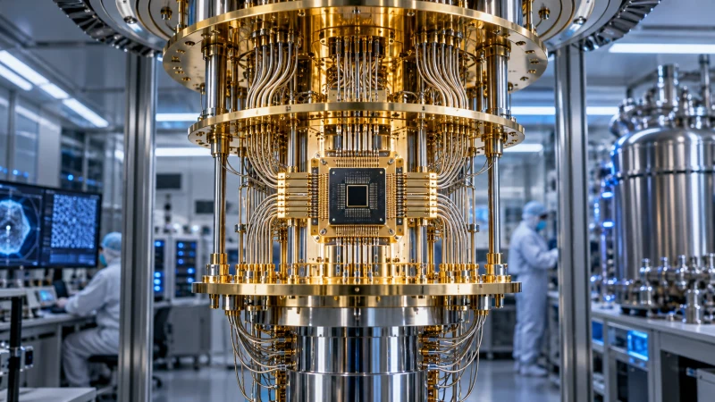
The U.S. Department of Commerce has finalized a CHIPS and Science Act R&D award of up to $1 billion for Anderon, IBM’s quantum foundry in Albany, New York. IBM is matching the award with another $1 billion in cash and is adding intellectual property, assets and skilled workers to scale production of quantum wafers on a 300 mm line.
Read more →
·
Wafer Fabrication
October 7, 2026
Companies & Market
Infineon Technologies has inaugurated a new backend manufacturing site in Bangkok, Samut Prakan, to expand its global production footprint and add capacity for future growth. The greenfield facility is designed for scalable high-volume output, with cleanroom, assembly, test and wafer test capabilities supported by advanced automation.
Read more →
·
Assembly

October 6, 2026
Supply Chain & Sites
Reports of a possible TSMC collaboration with Elon Musk’s “Terafab” plan are already reshaping expectations in Taiwan’s semiconductor facility engineering supply chain. Some contractors are drawing up Texas strategies, while others have begun establishing local offices before any official TSMC announcement.
Read more →
·
Fundamentals
October 6, 2026
Devices & Products
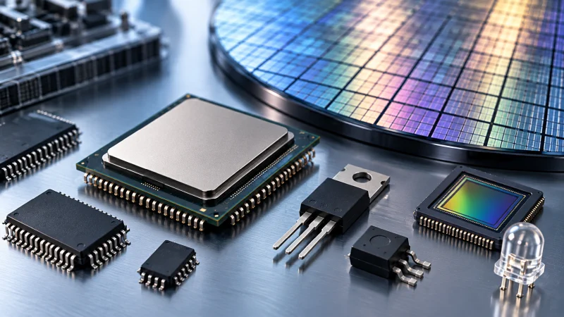
Continuity testing is the first step in a semiconductor test flow. It verifies that the DUT is correctly connected to the ATE by checking for opens and shorts and by using the expected behavior of the device’s ESD protection diodes to confirm the pin path.
Read more →
·
Wafer Test
October 6, 2026
Industry & People
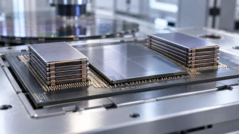
South Korean memory makers are reportedly quoting much higher long-term contract prices for sixth-generation high-bandwidth memory. HBM4 is expected to sell for about US$500 to US$550 in 2026, while 2027 quotes could reach US$1,400 to US$1,600, reflecting a 1.8x to 1.9x increase.
Read more →
·
Fundamentals

October 6, 2026
Research
imec has outlined a scalable sCFET architecture that combines split-gate and common-gate options without sacrificing area efficiency. The work also introduces a 5T+1 CFET SRAM bit cell and improves back-end-of-line routability for dense standard cells.
Read more →
·
Fundamentals
October 6, 2026
Devices & Products
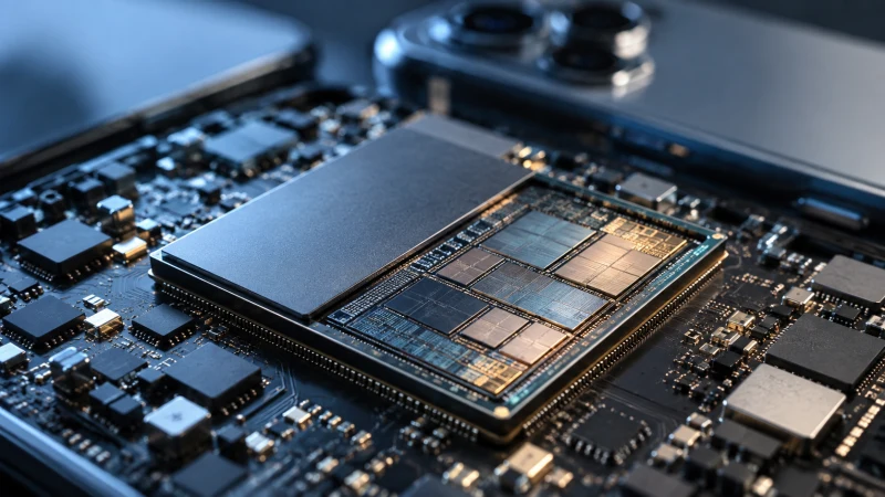
Samsung Electronics has reportedly started front-end wafer mass production of the Exynos 2700 mobile application processor. Planned output is set at more than 10% above the Exynos 2600 as Samsung prepares broader use of its in-house chips across the Galaxy S27 lineup.
Read more →
·
Fundamentals
October 6, 2026
Research
Researchers from ETH Zürich, CISPA, and New York University have proposed Terracotta, a framework that pairs custom DRAM command extensions with a programmable memory controller. The approach is designed to reduce the repeated redesign effort that has slowed the deployment of techniques for in-DRAM computation, lower latency, higher parallelism, and improved maintenance and reliability.
Read more →
·
How does it work?
October 6, 2026
Research
Researchers from Seoul National University and Yonsei University have demonstrated a monolithically integrated memristor-thin-film transistor kernel for multimode reservoir computing. By vertically combining Ru/HfO2/TiN memristors with In2O3 channel TFTs, the structure allows the temporal conductance dynamics to be tuned electrically across a broad time scale.
Read more →
·
How Does It Work?
October 6, 2026
Companies & Market
Applied Materials and Intel are deepening their collaboration on next-generation transistors, interconnects and advanced packaging for AI computing. The work combines Applied’s EPIC Center in Silicon Valley with Intel’s R&D campus in Hillsboro, with the stated goal of shortening the path from lab-scale development to high-volume manufacturing.
Read more →
·
Advanced Packaging
October 6, 2026
Research
A new technical roundup highlights work on low-contact-resistance WSe₂ transistors, backside clock meshes for 2nm GAAFETs, row-parallel DRAM processing, HBF for high-throughput LLM serving, formal CAN XL security analysis, and methods for abstraction and validation from physical devices to RTL.
Read more →
·
Devices