Short updates from the semiconductor industry, with context and links to the relevant chapters.

October 19, 2026
Research
Researchers from UC Berkeley, Samsung Electronics, and Intel have reported a nanoelectromechanically gated gain-cell eDRAM design that addresses three long-standing drawbacks of gain-cell memory: limited retention, parasitic coupling, and boosted write-voltage requirements. The approach targets the density and energy-efficiency advantages of gain cells while trying to remove the mechanisms that have kept embedded DRAM from scaling more cleanly.
Read more →
·
Devices
October 18, 2026
Research
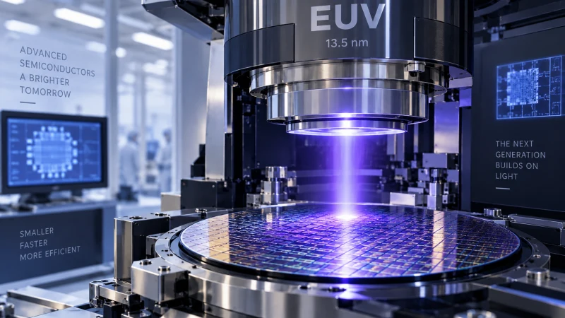
Maskless EUV lithography could offer a middle ground between serial electron-beam writing and conventional masked EUV. Instead of relying on a custom photomask, a programmable optical element would project digital patterns directly onto the wafer, with the aim of reducing mask cost and shortening design iteration cycles for low-volume and rapidly changing chip designs.
Read more →
·
Photolithography
October 16, 2026
Industry & People
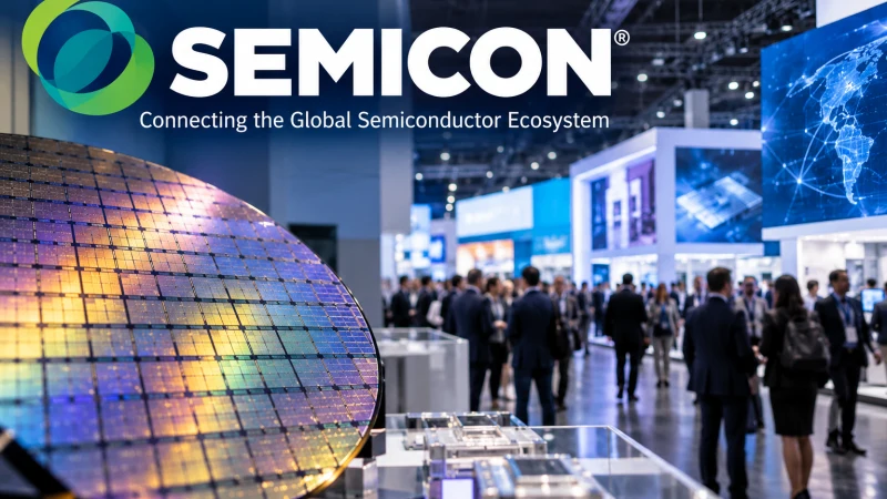
SEMICON West 2026 in San Francisco framed semiconductors as a trillion-dollar industry and put AI at the center of the next fab buildout. The show highlighted new inspection tools from ZEISS, panel-level packaging deposition from Von Ardenne, motion-control equipment from Heidenhain, materials work from Mitsubishi Chemical Group, and workforce programs led by ABM.
Read more →
·
Wafer Fabrication
October 16, 2026
Industry & People
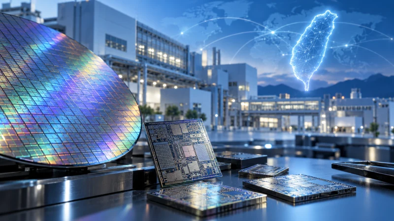
At iTechCon 2026, industry and research speakers argued that AI value is shifting from standalone chips toward co-design across hardware, models, software, packaging, and system architecture. The discussion highlighted Taiwan’s strengths in semiconductor manufacturing and advanced packaging, but also its need to deepen software capability, cross-disciplinary talent, and startup support as AI moves into inference, agentic AI, edge devices, and physical AI.
Read more →
·
How Does It Work?
October 16, 2026
Companies & Market
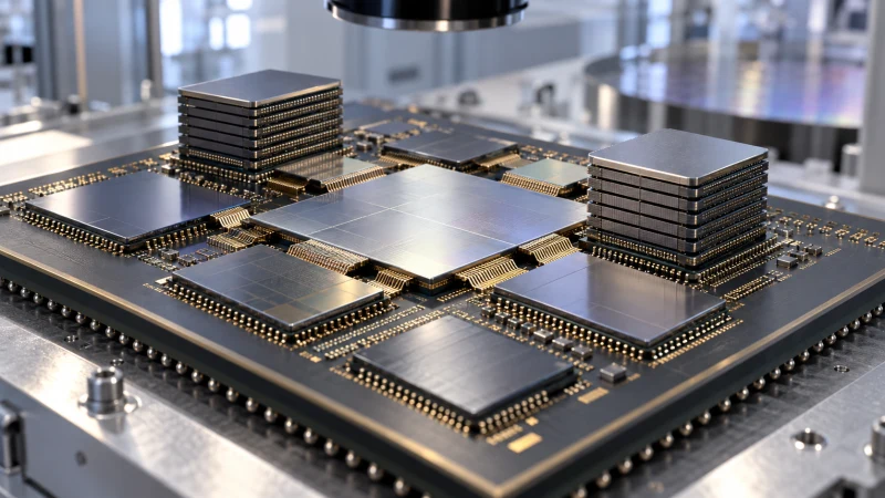
Patent filings analyzed by SemiAnalysis suggest that ASML is preparing a die-to-wafer hybrid bonder, signalling a second step beyond lithography into advanced packaging. The tool would place ASML in direct competition with Besi and with other front-end equipment makers that are targeting the same packaging market as transistor scaling becomes more difficult and expensive.
Read more →
·
Advanced Packaging

October 16, 2026
Industry & People
A dense week in semiconductors brought fresh fab expansion, new packaging and test initiatives, stronger AI-related spending signals, and continued momentum in China’s memory and EUV efforts. TSMC and ASML both reported strong quarters, while startups in photonics and 3D compute secured new funding and quantum hardware teams posted notable technical progress.
Read more →

October 16, 2026
Companies & Market
TSMC said demand for CPUs tied to agentic AI continues to rise even as overall AI demand remains very strong. The company also pointed to advanced packaging and silicon interposer capacity as critical constraints, while higher costs from new fabs and N2 ramp-up continue to weigh on margins.
Read more →
·
Advanced Packaging

October 16, 2026
Supply Chain & Sites
TSMC and GlobalFoundries are drawing attention to a fast-expanding market in which mature wafer processes support advanced packaging rather than leading-edge logic. Silicon interposers, through-silicon vias, and embedded deep trench capacitors are emerging as the main demand drivers for this capacity, creating a sizable opportunity around older process nodes.
Read more →
·
Advanced Packaging
October 16, 2026
Research
Langdao Silex (Shanghai) Technology has publicly presented an extreme ultraviolet light source prototype rated at 15 W and described as 90% localized. The debut marks a step in domestic lithography development in China, but the system is still reported to be three to five years away from mass production, with output power and long-term stability remaining the main engineering hurdles.
Read more →
·
How Does It Work?
October 15, 2026
Research
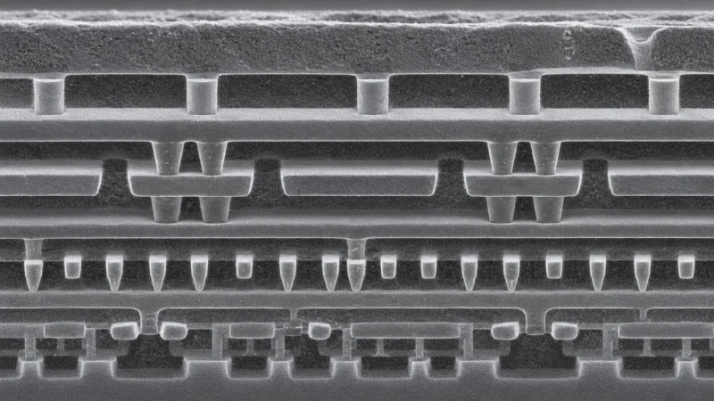
As designs move into sub-5nm nodes, vias have become a major weak point in the interconnect stack. Automated, signoff-aware via insertion shifts optimization into implementation, adding redundant vias to reduce resistance, improve IR drop behavior, and strengthen electromigration margins while avoiding late-stage ECO loops.
Read more →
·
How Does It Work?
October 15, 2026
Companies & Market
Infineon has signed a supply agreement with Wolfspeed for 200 mm silicon carbide wafers, adding another step to its effort to strengthen supply chain resilience for SiC-based power devices. The agreement centers on wafer supply rather than finished components and points to continued scaling in the silicon carbide value chain.
Read more →
·
Compound Semiconductors
October 15, 2026
Research
Ayar Labs and GUC report thermal co-simulation results for a multi-chip package that combines optical engines with high-power AI processors. A liquid-cooled cold plate met the temperature targets, while a standard air heatsink failed to keep the package within spec.
Read more →
·
Optoelectronics & Photonics
October 15, 2026
Research
Researchers at ETH Zurich and New York University have published a detailed experimental study of power consumption in real HBM2 DRAM chips. The work identifies strong operation-dependent and data-pattern-dependent variation, with read operations drawing more current than any other access and specific bus toggling increasing power by 29.4% under the tested conditions.
Read more →
·
Fundamentals
October 15, 2026
Companies & Market
ASML is no longer simply accepting demand for its extreme ultraviolet lithography systems. The company says customers are already looking to place orders for 2029 and 2030, but these requests will be weighed against ASML’s available capacity before any allocation is made. At the same time, ASML confirmed that customers have agreed to pay more for its most critical EUV machines.
Read more →
·
Photolithography
October 15, 2026
Companies & Market
Two major memory chipmakers have reportedly agreed to higher replacement-part prices from ASML, even as the lithography supplier prepares broader price increases for its most critical tools. The focus now shifts to TSMC, ASML’s largest customer, which had previously been described as resisting such hikes.
Read more →
·
Photolithography